
No More Missing 3D Bodies: Generating Precision PCB STEP Models from Datasheets with SolidCraft MCP
How to use SolidCraft's Model Context Protocol (MCP) and LLMs to turn 2D component datasheet drawings into production-grade 3D STEP models for KiCad in minutes.
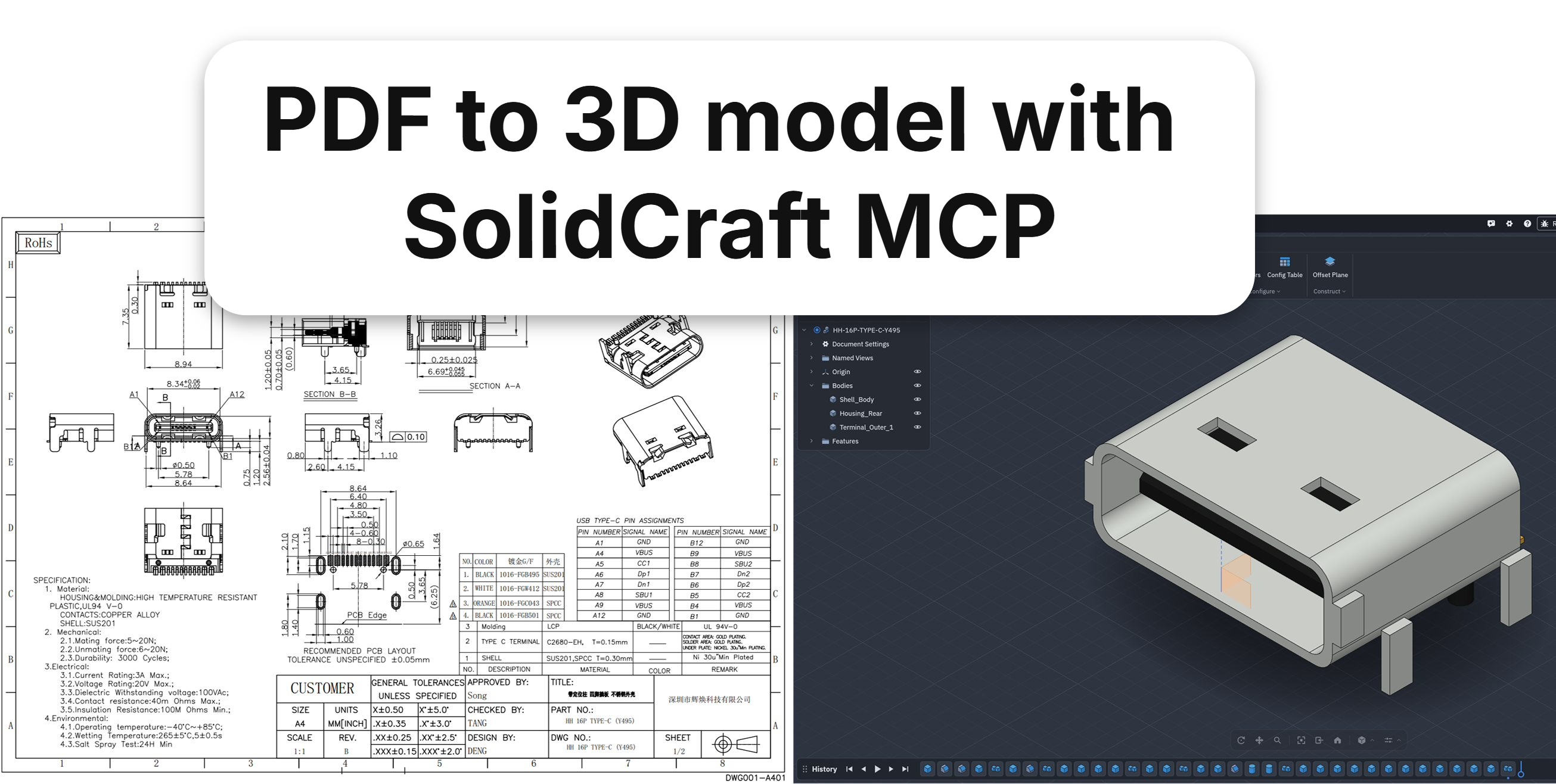
During modern PCB layout, 3D visualization is no longer just a visual gimmick—it is a critical design verification phase.
In KiCad, inspecting your board in 3D is essential for catching spatial and mechanical interference before ordering prototypes:
- Ensuring tall electrolytic capacitors or inductors don’t collide with enclosure lids.
- Verifying that right-angle connectors sit flush with front-panel cutouts.
- Checking component-to-component clearances around heat sinks and daughtercards.
- Downstream rendering in Blender (via
pcb2blender) to produce photorealistic marketing assets, documentation, and user manuals.
The moment a component lacks a 3D model, the entire board visualization breaks.
A missing 3D body leaves bare copper pads floating on the substrate. The traditional workaround—assigning a colored generic bounding box—is sloppy and deceptive: a rectangular block cannot verify connector mating depth, shield flange overhang, or alignment of plastic locating pins.
Here is how I eliminated the missing 3D body bottleneck entirely by pairing component datasheets with SolidCraft and the Model Context Protocol (MCP).
The Supply Chain Reality: Missing CAD Assets
Tier-1 component manufacturers (such as Texas Instruments, Molex, or TE Connectivity) almost always provide downloadable 3D STEP or IGES files.
However, hardware engineering increasingly relies on cost-effective, specialized, or second-source components from distributors like LCSC or JLCPCB’s parts library. While these components are electrically solid, their product pages rarely feature downloadable 3D models:
- GrabCAD / 3D ContentCentral: Searching community databases is a gamble. You might find a model that looks similar, but subtle differences in shield tabs, locating boss diameters, or pin pitch often lead to mechanical fit errors.
- Manual CAD Modeling: Opening Fusion 360, SolidWorks, or FreeCAD to model a complex connector takes 30 to 60 minutes of repetitive sketch-and-extrude operations—time you rarely have during an active PCB layout sprint.
Yet every single legitimate component datasheet shares one invariant: the 2D mechanical dimension drawing.
The package tolerances, pin pitches, locating post positions, body heights, and shell cutouts are already fully documented. The only missing link was an automated, programmatic bridge from dimensioned drawing to parametric CAD.
Enter SolidCraft & the Model Context Protocol (MCP)
SolidCraft is an independent, parametric 3D CAD application (conceptually similar to Fusion 360 and Onshape) featuring a native Model Context Protocol (MCP) connector.
Through its MCP server, an LLM gains direct programmatic control over a full-featured parametric CAD modeling kernel:
- Executing exact 2D sketches, geometric constraints, and dimensions.
- Building solid primitives and complex features (
solid.box,solid.cylinder,solid.hole,solid.fillet,solid.shell). - Running CSG boolean operations, edge chamfers, and linear/radial patterns.
- Performing closed-loop topological inspection (
inspect_design,measure,body_topology) to verify volumes, center-of-mass, and bounding box dimensions. - Exporting native, watertight AP214 STEP (
.step) files.
Instead of fighting CAD GUI menus, I hand over the mechanical dimension drawing directly to the LLM. The model parses the dimensions, executes the parametric commands through SolidCraft MCP, verifies the bounding geometry, and spits out an exact STEP file ready for KiCad.
Case Study: 16-Pin USB Type-C Receptacle (LCSC C52209111)
To test the workflow on a non-trivial component, I tackled a common right-angle SMD USB Type-C connector: the HH 16P TYPE-C (Y495) (LCSC Part C52209111).
This connector features intricate geometry:
- A stamped stainless-steel outer shield with chamfered lead-in edges.
- A molded internal plastic tongue with 16 SMT signal contacts.
- Four through-hole shield retention legs designed to anchor into the PCB.
- Two bottom plastic locating posts for pick-and-place orientation.
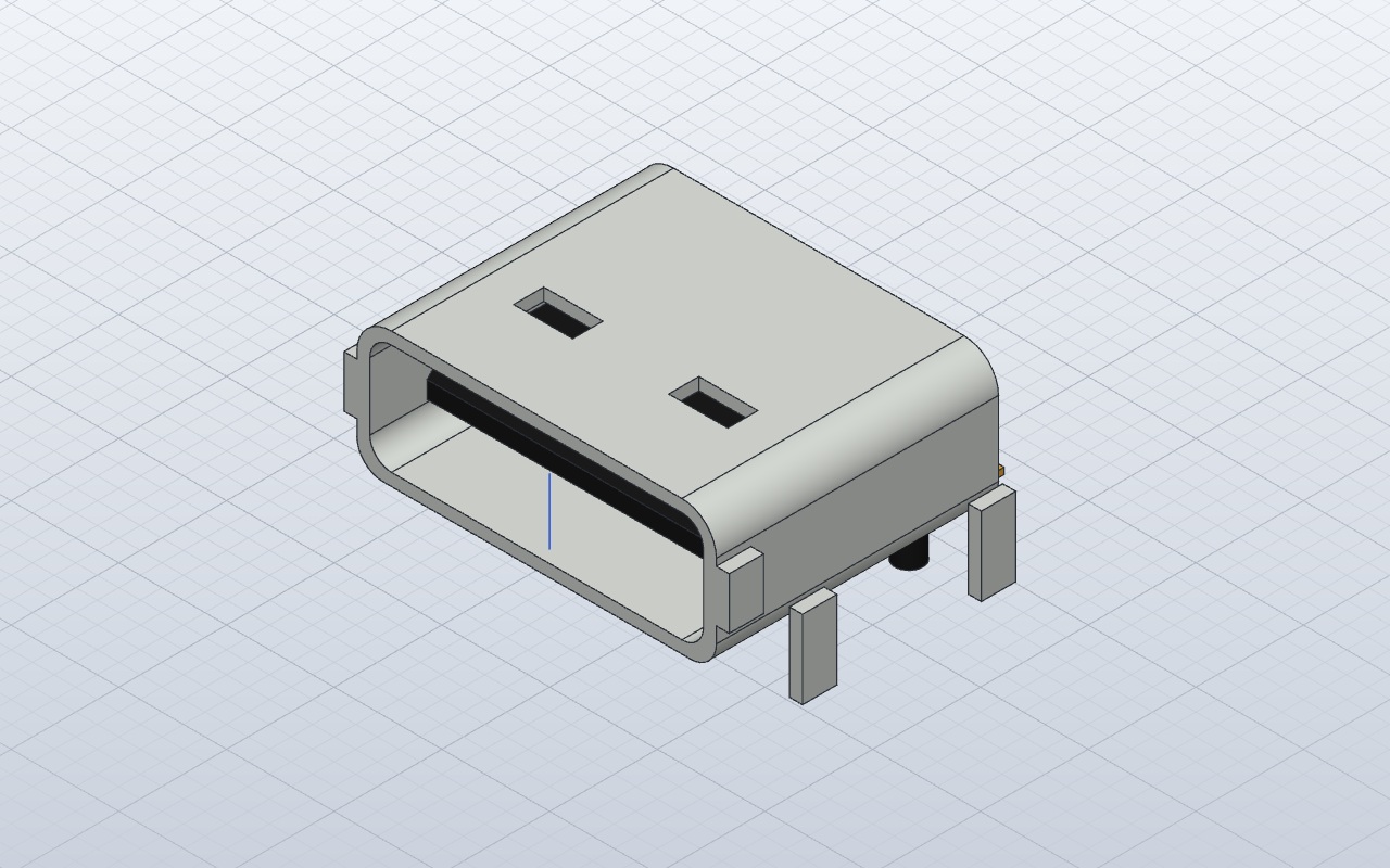
1. Dimension Extraction
From the manufacturer’s datasheet drawing, the key mechanical specifications are extracted:
- Body Width & Depth: $8.94\text{ mm} \times 7.35\text{ mm}$.
- Overall Height: $3.26\text{ mm}$ above the PCB plane.
- Port Opening: Standard Type-C oval profile ($8.34\text{ mm} \times 2.56\text{ mm}$ with $R = 1.28\text{ mm}$ full-radius end caps).
- Shield Standoff & Legs: $4\times$ through-hole solder tabs ($0.80\text{ mm} \times 0.30\text{ mm}$) with front-to-back spacing of $5.50\text{ mm}$.
- Locating Bosses: $\varnothing 0.65\text{ mm}$ plastic posts extending $0.60\text{ mm}$ below the seating plane.
2. Parametric Construction via MCP
The LLM plans the model hierarchically and passes batch commands to the SolidCraft kernel:
// Example: Creating the outer Type-C stamped shield profile
{
  "command": "solid.box",
  "name": "ShieldBody",
  "width": "8.94",
  "length": "7.35",
  "height": "3.16"
}
Next, it applies outer edge chamfers to replicate the stamped metal lead-in, shells the internal cavity, inserts the internal dielectric tongue ($0.70\text{ mm}$ thickness centered along the receptacle axis), and extrudes the bottom retention legs and alignment pins at their exact coordinate offsets.
3. Automated Topological Verification
Before exporting, the model queries SolidCraft’s verification tools:
measure: Validates that the outer bounding box matches the datasheet within $\pm 0.05\text{ mm}$.body_topology: Verifies cylinder centers and radii for the locating posts.
Once verified, calling export {"format": "step", "path": "USB_Type-C_16P_C52209111.step"} produces a standardized, AP214 color-capable STEP body in seconds.
Integrating into the KiCad Footprint
With the STEP file generated:
- Open the component footprint in KiCad’s Footprint Properties (
Ctrl+Ein Pcbnew). - Navigate to the 3D Models tab.
- Add the generated model using a project-relative path:
${KIPRJMOD}/3dmodels/USB_Type-C_16P_C52209111.step - Adjust the coordinate offset so the bottom seating plane aligns with the footprint surface ($Z = 0$) and the locating posts snap into their non-plated PCB drill holes.
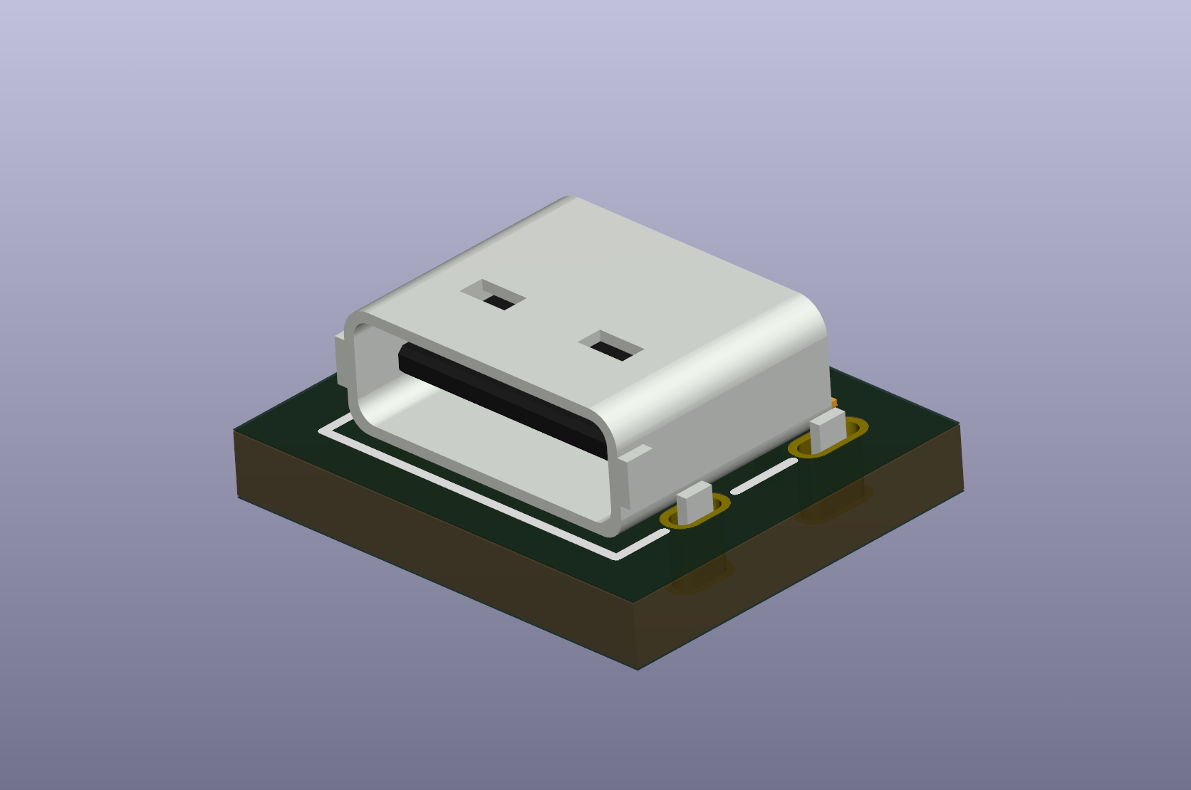
The connector now aligns perfectly with the silkscreen outline, the solder pads sit centered under the SMT contact leads, and the shield tabs extend cleanly through the PCB slots.
The New CAD Reality
For years, hardware designers have accepted missing 3D models as an annoying, unavoidable friction point in the PCB design process. We settled for flat 2D views or spent evenings drawing dummy boxes in mechanical CAD.
By connecting LLMs to a native parametric CAD kernel through MCP:
- The mechanical dimension drawing on the datasheet becomes the only input needed.
- Accurate, watertight, production-grade 3D bodies are generated in minutes.
- Enclosure clearances, front-panel fitment, and photorealistic board renderings work out of the box.
The era of missing PCB 3D models is officially over.