Tuning a PCB Antenna in the Loop, From KiCad to a 3D-Printed Radiation Pattern
I’ve been closing the loop between KiCad and openEMS for antenna tuning, no manual coordinate transcription, no guesswork. Edit the copper in KiCad, simulate, read the dip, repeat.
The antenna: a 2.4 GHz meandered inverted-F (IFA), copper artwork adapted from TI’s DN007 reference design, feed leg, shorting stubs down to a ground pour, single top-layer trace.
The sim
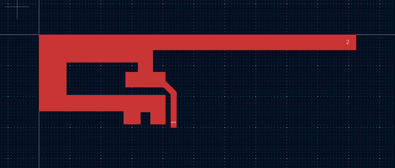
openEMS (FDTD) via its Python bindings: substrate + copper as simulation primitives, PML boundaries (a radiating structure reflects too much off the cheaper absorbing-boundary option), a lumped port bridging the feed leg to ground, and a near-field-to-far-field box for the radiation pattern.
The KiCad round-trip is the part I actually wanted: import the copper polygon straight from the footprint, the importer works out the feed leg (whichever leg reaches furthest toward the ground pour) and the pour edge on its own, no manual bookkeeping between the drawing and the sim model. Tune the shape in KiCad’s footprint editor, re-run, read S11, export back out once it’s dialed in.
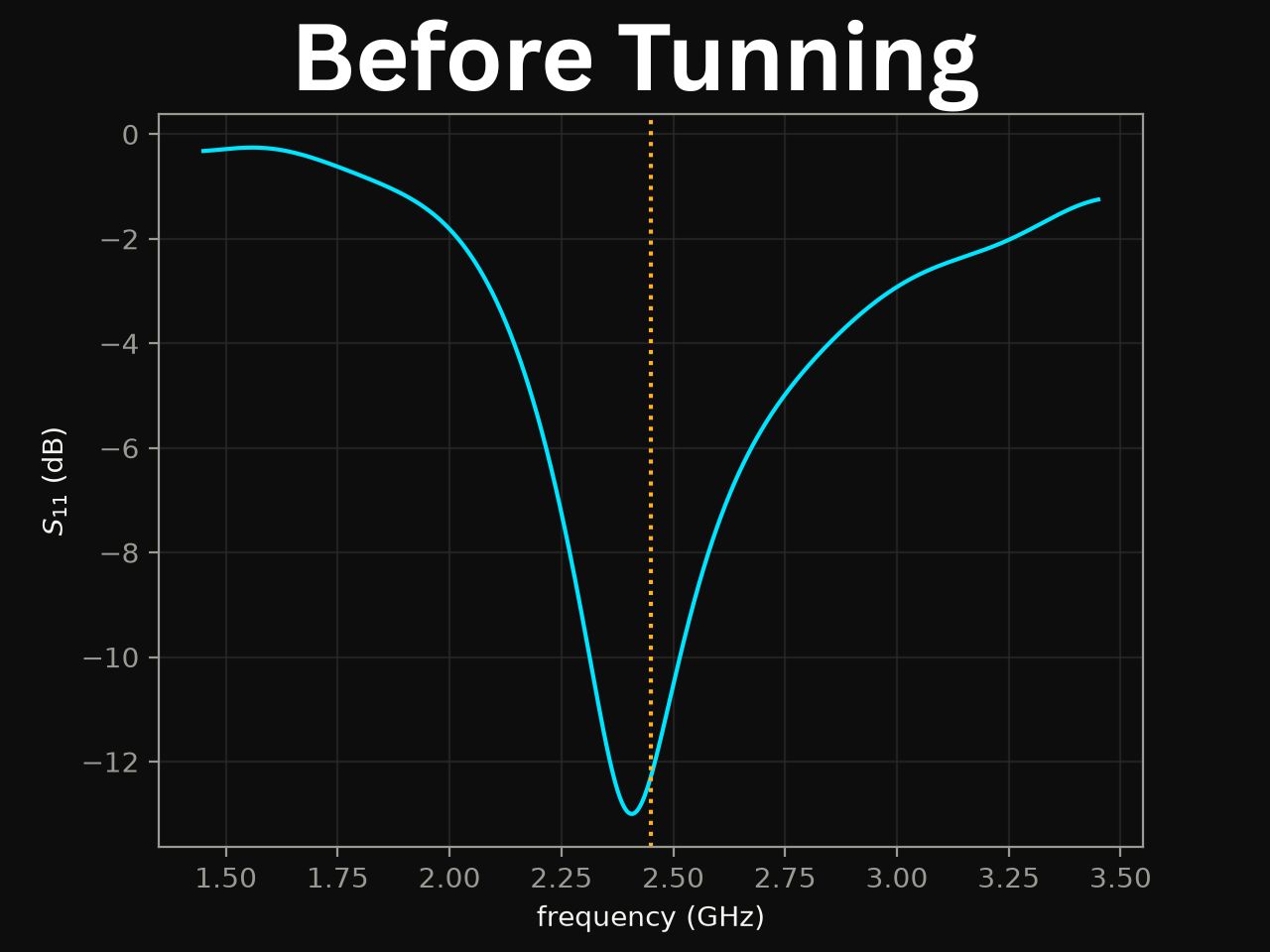
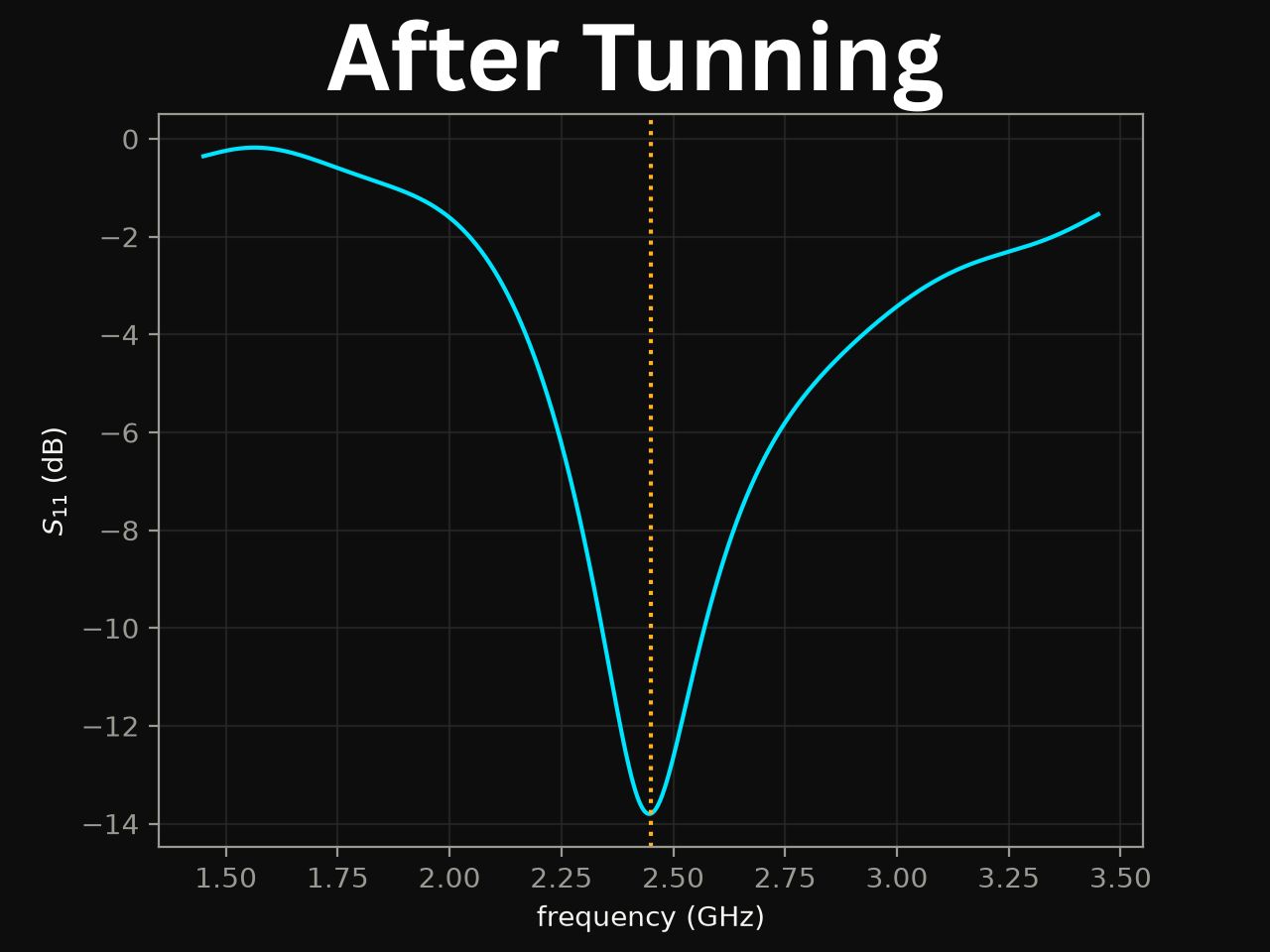
Baseline (untuned, verbatim reference artwork): −13.0 dB at 2.407 GHz, already under the −10 dB bar, about 43 MHz shy of 2.45 GHz. Trimmed the radiating arm roughly half a millimeter to walk the dip up to target.
Seeing the pattern
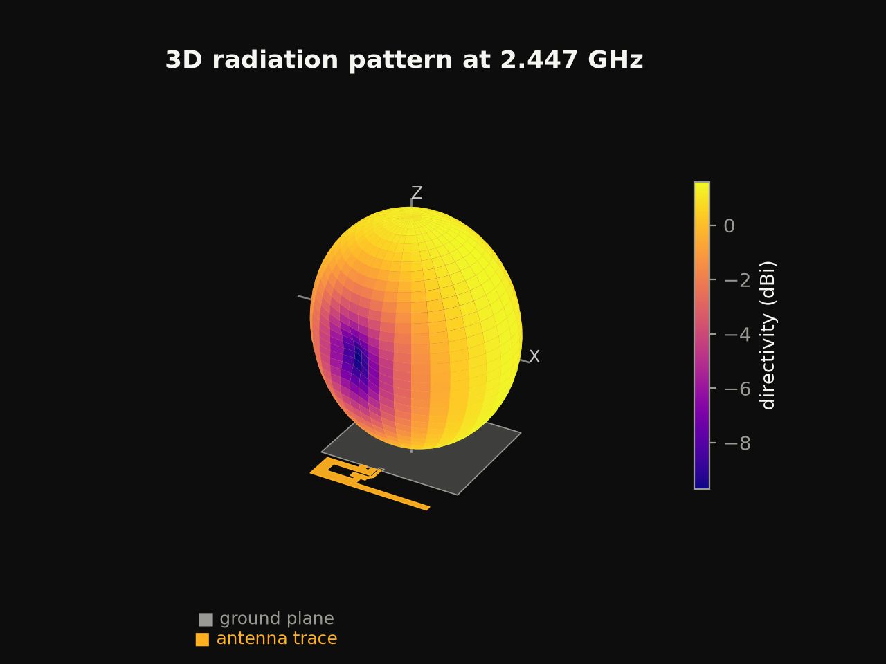
Past S11/Zin, the far field: two great-circle cuts at the S11 minimum for a quick look, and, because two 2D slices only tell you so much, a full-sphere sweep (~2600 look directions) rendered as an actual 3D directivity surface, with the antenna’s own footprint dropped in underneath for orientation.
Printing it
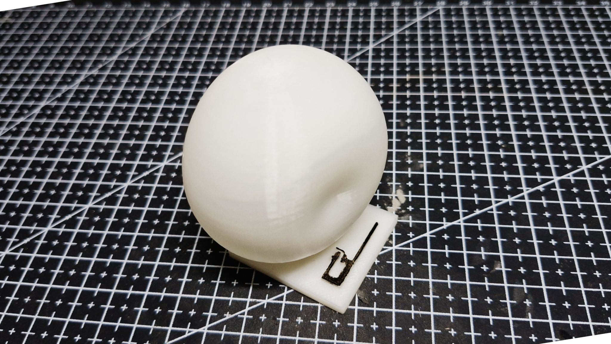
The part I didn’t expect to end up doing: turning that far-field sweep into something you can hold. The same spherical (angle, angle, gain) grid that feeds the plot triangulates cleanly into a watertight mesh, cap the two poles with a single averaged point each (they’re literally the same physical direction sampled once per azimuth, and floating-point noise between those samples is the only thing keeping the mesh from closing exactly), scale the peak-gain radius to something print-sized, done.
One problem: a shelf of these from different tuning passes all look identical once they’re just white plastic blobs. So there’s a second object, a small plaque of the actual board at true size, with the antenna trace itself raised on top (rasterized onto a fine grid rather than triangulated, since a meander is about as far from convex as a shape gets), so each print carries its own identity. It’s a separate STL rather than fused to the lobe: sinking a flat base into the sphere is geometrically fine, but the two shells then genuinely intersect, and slicers tend to choke on that. Cleaner to print both and place them by hand.
Takeaway
No single piece of this is the interesting part, it’s that the whole chain, copper artwork → S11 → far field → physical object, stayed scriptable end to end. Change the artwork, and everything downstream just flows through without retyping a single coordinate.