Carrier board design - Part 3
Welcome to part 3 of the series of carrier board design
I know we have not even started to talk about the carrier board design, we are first covering the fundamentals that will be essential to understand the thing we do in design. Here is a link to part 1 and part 2
Today we will talk about time and distance
Time and Distance
The EM wave travels at speed of light in vacuum, but on the PCB, the dielectric slows down the signal. Just as light slows down when it enters glass or any other medium with index of refraction greater than 1. Here is the equation for speed of EM wave.
\[ V = \frac{c}{\sqrt{\epsilon_r}} \]where:
- \( V \) is the velocity of the electromagnetic wave,
- \( c \) is the speed of light, and
- \( \epsilon_r \) is the permittivity of the medium.
It takes roughly 1ns to travel 15 cm in PCB trace, with \( \epsilon_r \) of 4.6
High speed does not imply high frequency as many would assume, I did. It’s related to the rise and fall times of the signal or fast edges. So, you could have a high-speed circuit that may be running as low as 1Hz. But by inherent time period of high frequency, the rise and fall time fall (no pun intended) under high-speed domain.
The signal switches so quickly that the transition is complete before the signal can travel to the other device through the trace.
Now the PCB traces work as transmission lines.
The below animations shows how the signal travels in a high vs low rise time.
High Rise time
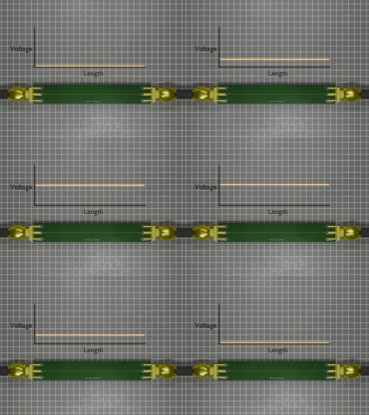
Low Rise time
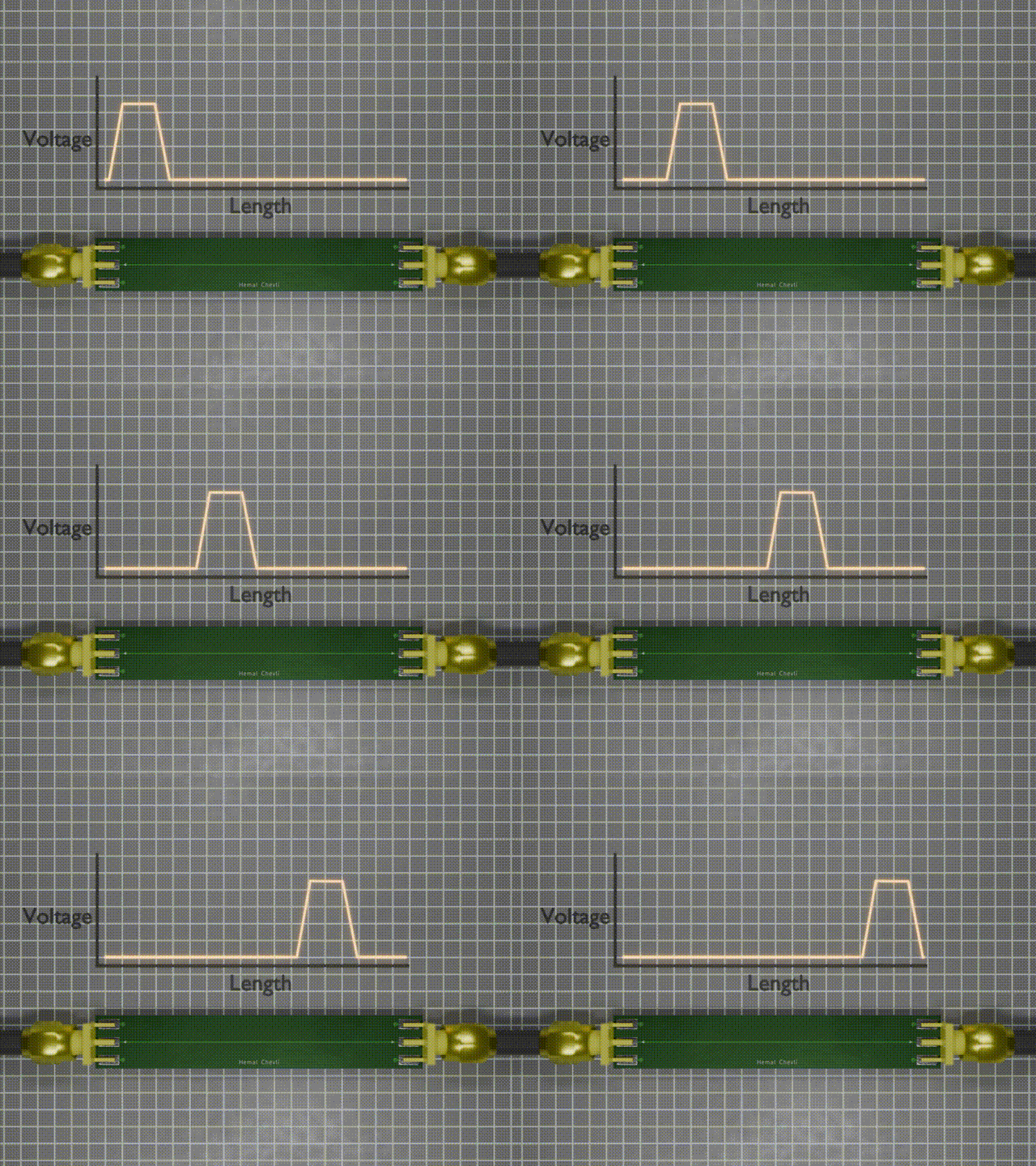
Rise and fall times
The energy is concentrated on the edges and the skin effect comes into play where the signal travels on the surface of the copper trace.
Now I won’t go into the math of the transmission, but I’ll touch upon the concept of Fourier series.
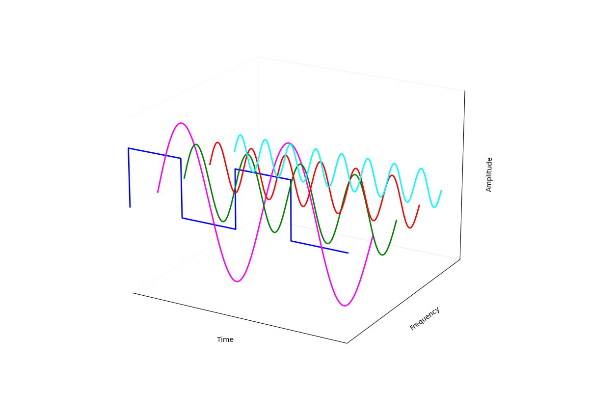
The square waves are constructed as sum of sine waves of different frequencies and amplitudes.
So, the higher the rise time, there are more and more sine components present in the wave. So sometimes even when you are running at a certain frequency you can find it may be causing interference at a higher frequency, these are the harmonics of the fundamental frequency.
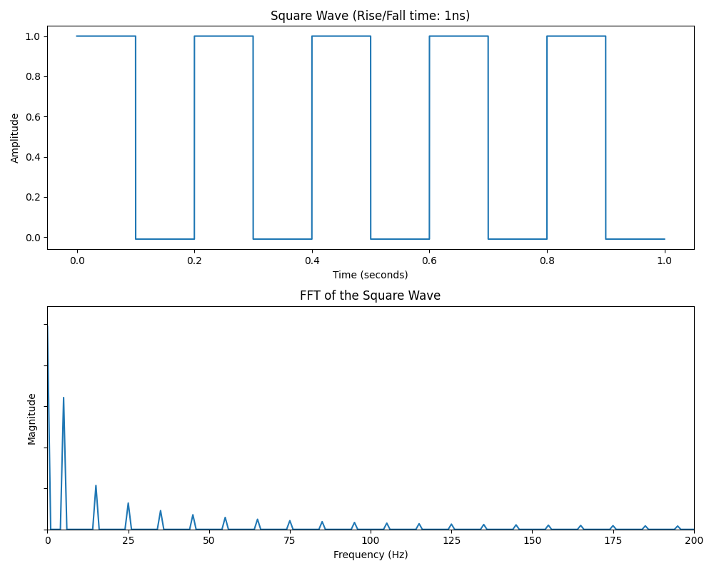
Turns out there was a silicon revision which had smaller gates that made the rise and fall times smaller.
So how does the signal rise time and fall is affected on a physical level.
Let’s look at a simple NOT gate.
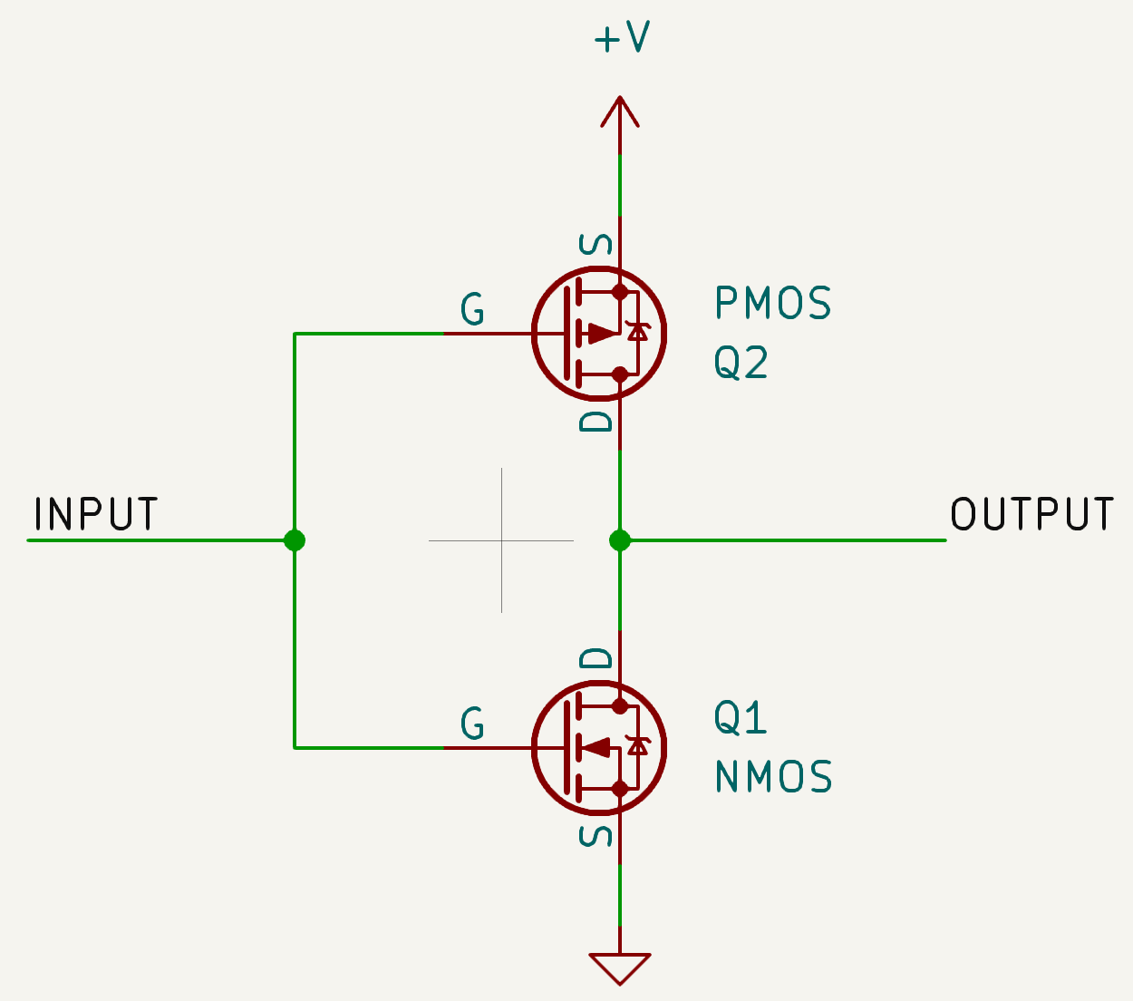
This comes down to the physical size of the MOSFET.
How quickly the channel opens dictates the rise and fall time. The time to open and close the channel depends on how quickly the gate of the MOSFET is charged. The gate of the MOSFET is essentially a capacitor. The time to charge the capacitor depends on the area of the two plates and the voltage level. So, the smaller the physical size of the gate of the mosfet and lower the voltage to which the capacitor needs to be charged, the less the rise and fall time of the signal.
There are other components that affect the rise and fall times including Inductance of the package lead, drain current etc.
I share a real-life example; a company was making some automotive PCB for a long time and everything worked without any problems. Then suddenly they started to have EMI issues in the whole batch. They were running the system at 8MHz or thereabouts, but they measured frequencies in the range of several hundred MHz What happened was the IC they were using underwent a silicon revision to a smaller process. This led to quicker rise and fall times, and the PCB had to be redesigned to account for this.
In electronics we are constantly pushing the limits to make things work faster on devices. To do this, we need to send data to and from CPU and memory. The faster the data is present and processed and sent back the quicker the system. So, we need to increase the bandwidth of the information.
This is the reason faster signals have lower transition voltage, e.g. DDR4 RAM has 1.2V. The picture below depicts this, with the same rise and fall slope, by decreasing the voltage level, you shorten the rise and fall times of the signals.
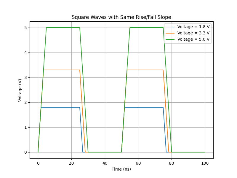
Many ST chips offer the edge speeds to be set via firmware. If you are not sure which to use, you should be fine with the slow signal. This will at least cause the least EMI problems, and it will work at the frequency you set, again using the slow signal setting does not mean that you are using slow frequency. Slow and fast does not mean the frequency.
High frequency in GHz range, always have faster rise and fall times. Low frequency can have both slow or fast rise time and fall times.
Let’s look at an example, There is a 1 Hz signal with 100ms of rise time. This is possible.
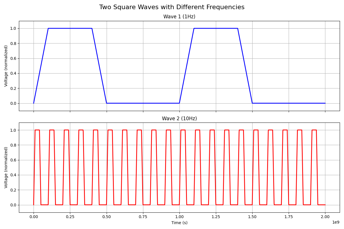
But if we take a 10 Hz signal that has a period of 100ms, it’s not possible for this 10 Hz signal to have 100ms rise time. It must be in order of 1-2 ms or less. If we try to do this the square wave will essentially turn into a triangle wave.
So as the frequency increases, inherently the rise and fall time get shorter.
Next week we will talk about reference planes and reflections.
And as always, all the content is OG and no LLM’s or diffusion models were used in this post.
Archives
Tags