Carrier board design - Part 4
The question is when is your design a high-speed design?
When the trace length is greater than ¼ of TEL, the design is high speed, and care must be taken to maintain signal integrity.
So, what is TEL?
It stands for Transition Electric Length. Let’s understand with an example. Say a signal has a rise time of 1ns. Now we know on a PCB, signal travels 15cm in 1ns. So, TEL of 1ns rise time signal is 15cm. ¼ TEL is 3.75cm. So, a signal with 1ns rise time has a trace length of more than 3.75cm, the design is high speed, and we need to think about the signal integrity. TEL is the length a signal travels in the given rise time.
Ground and Power planes.
I prefer to use the term reference planes, there are no ground plane in electronics on aircraft, right? And also, because the term ground has a wide variety of meanings in electronics. There is AC ground, chassis ground, negative terminal of power supply is called ground, and, in our case, the other half of the transmission line is also called ground.
When we are drawing the schematic, we draw signals traveling from source to sink. But on the pcb this is just half the story. On PCB the signal goes from source to sink and comes back to source via the reference plane. Now again it’s not the signal goes from point A to B and then comes back from B to A. Forward and return currents occur simultaneously.
In high-speed design, it is not necessary to route signals only above DC ground plane, one can use any power plane. But care must be taken when switching signals between power planes, but that is for another post.
The return path follows the path of lowest impedance. Key work here is impedance. When the rise times are slow, the return path is ohmic and follows the path of least resistance, which is just a straight line from source to sink.
But as the rise time increases, the above path has higher impedance, and the signal mirrors just below the signal trace on the reference layer, as this is the path of least impedance.
When there are breaks in the reference plane, the return current spreads out and current flows in the ref plane changing its voltage at a certain place and this unwanted current causes metastability in the circuit.
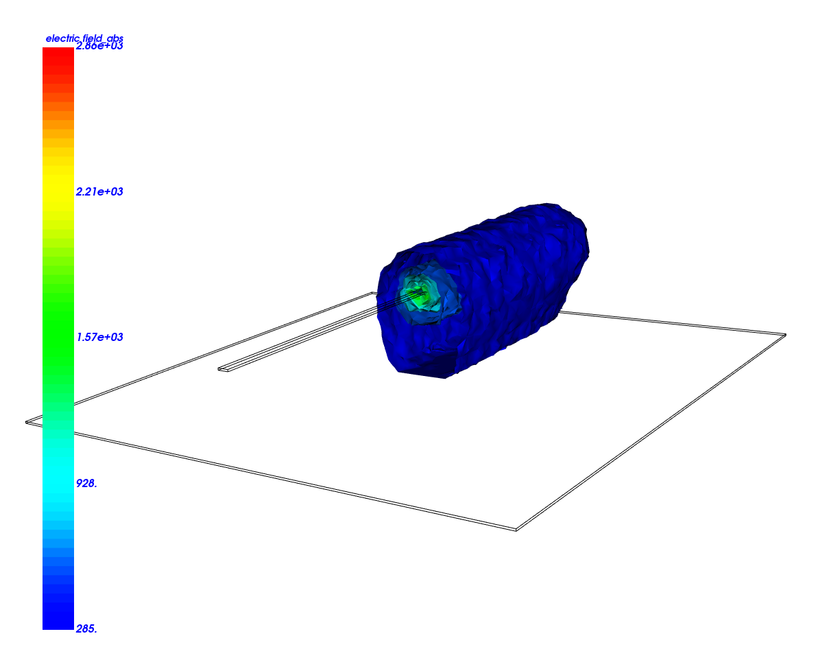
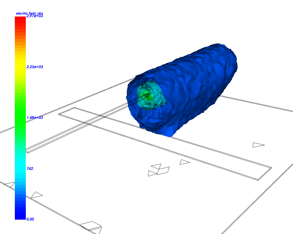
Below is a simulation of static electric fields of a trace over a solid reference plane vs a plane with a slot.
As you can observe, the electric field is stronger near the slot.


Impedance
At DC or low frequencies, the major component of impedance is resistance, at a few kilohertz, the reactance components come into play.
\[ Z_0 = \sqrt\frac{L_0}{{C_0}} \]Above is a simplified equation of the characteristic equation. Notice the impedance is not a function of length of the transmission line. Also, the impedance of the line is not a function of frequency. As long as the geometry of the trace does not change and the dielectric constant doesn’t change with frequency, the impedance will remain constant.
For most transmission lines in our case, the resistive component is negligible.
Reflections
This is one of the most interesting parts for me, I could go on into a separate blog series talking about signal reflections.
When an EM signal travels on a trace, it does so with very little loss. The losses come from parasitic resistance and dielectric losses. As soon as the signal encounters any change in the impedance of the line, some amount of energy is reflected back to driver, depending on the polarity the reflected signal will add or subtract to the signal.
I think controlling reflections in a transmission line is one of the most important things to control for signal integrity apart from cross talk and other effects.
Before we go into equations, I found the below video very helpful in intuitively understanding the reflections.
https://www.youtube.com/watch?v=DovunOxlY1k
The reflection formula is
\[ Reflection = \frac{Z_i-Z_o}{{Z_i+Z_o}} \]Where:
- \( Z_i \) is load impedance
- \( Z_o \) is output impedance
When the line is open at the end the voltage doubles, when its short circuited the energy is reflected inverted.
Stubs
Stubs are branches on a transmission line, these may be terminated or open, these can sometimes cause waveform reversals. This happens when the stub is a quarter of the wavelength of the signal.
It’s best to avoid them, especially when changing layers, or you need to add an expensive process of back drilling in the pcb production. Any branches of the transmission must have proper terminations.
LLMs were not used in creating this post nor diffusion models for creating images.
Archives
Tags