Open Source PCB Ruler
I’ve seen rulers from adafruit and EEV blog but I could not find the source files, so I could atleast print it out for my reference. So I’m making one, open source with CC-BY-SA license, CC-what. I’ll upload few pictures once I get things going. I’m yet to finalize the shape, I’m thinking the size of a credit card will work just fine. I’ll make a pdf as well so it can be printed and be used as a reference.
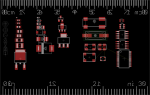
Here is a draft
Here are the foot prints I’m planning to add.
\[table\]RLC , IC
0201 , QFP 32 pin with different pitches 0402 , QFP 100 pin 0603 , BGAs 0805 , SSOP 1206 , SOIC 1210 , QIP 2010,
Diodes and transistors, Crystals sc79 , 5x3.2 sod323 , 3.2x2.4 sod80 , 2.5x2 s0012b , 2x1.2 sma ,hc49 smb , three pin smc, sc70 , Holes sot23 , 10 to 28 AWG and mm units( depends on real estate available) sot223, sot69 , Trace Widths dpak , Via Vs amp table d2pak , cm and in scale
Here is the GIT repository.
UPDATE(27-NOV-13): Added scales cm and in, on both sides.
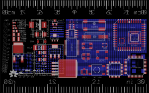
UPDATE(7-DEC-13):The foot prints are almost all there, I’m planning to add SMD prototype area on the back. And also make it more pretty
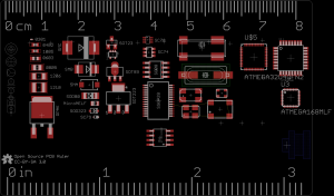
UPDATE(13-DEC-13) : Added trace width, colour code table, prefixes table, logo and AWG drill holes, and few footprints
UPDATE(14-DEC-13): I viewed the gerbers using free tool gerbV and also using a 3D gerber viewer, and found a few small issues with the pcb, some text was on wrong layer, a part name of an IC was present, the placement of holes was bit off, but all of that is fixed and here are the snapshots of top and bottom of the pcb
Archives
Tags


