PCB Fundamentals
Introduction
The older generation sometimes calls it a PW board (printed wire board).
Today we’ll have a bird’s eye view of a PCB. How it is designed, manufactured, tested and how it integrates into a product.
PCBs are hiding in all the electronics products we use, consumer electronics, IoT devices, drones, cars, etc.
Before PCB is made, there is usually a prototyping phase, where you’d make the design on a breadboard along with some dev board with a microcontroller on it. Once all the components and requirements are written down, the PCB design process starts.
What is a PCB?
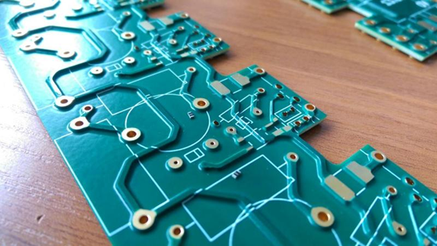
Let’s look at what the PCB is made of.
It’s made of layers of copper sandwiched between insulating material. The components like ICs, resistors, capacitors are then placed on the PCB and attached to the board by melting metal called solder, when it solidifies the two parts are connected.
These layers are called with slightly different names in the CAD packages.
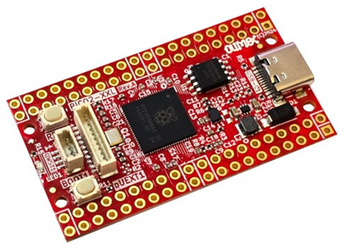
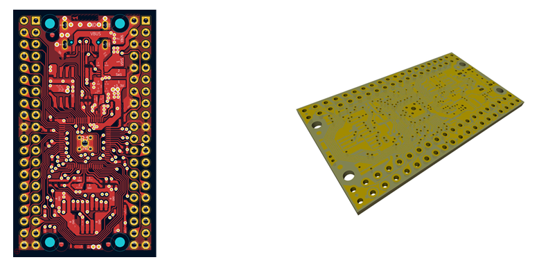
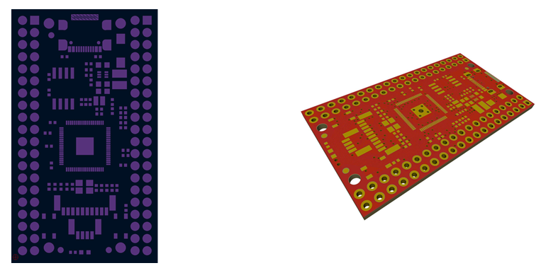
As an example we will take the open source product Pico2 XXL designed by Olimex.
The basic components are substrate, copper layer, prepreg, solder mask layer and silk screen.
Let’s look at each in detail.
Substrate
Sometimes also referred to as core, this is most of the time made of fiberglass, there other types of substrates like metal core PCB etc. This is what gives the PCB its rigidity.
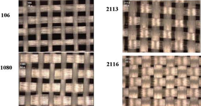
There are many different kinds of fiberglass, based on how tight the weave is. Some of the common weaves are called 1080, 2113. These basically tell us how tight the weave is. For boards needing impedance matching, the tighter the weave the better. There are substrates with different di-electric constants. This affects the speed of signal propagation on the PCB.

The empty space in between the weaves is taken by epoxy, thus the glue holds the core together. In impedance controlled boards, because the dielectric of the epoxy is different from the dielectric of the fiberglass, it can create problems.
The substrate (cores) are available in various thicknesses, most common is 1.6mm.
The substrate also has another property called Tg (Glass transition temperature), This is the temperature at which the core will get rubbery. This is an important property to consider for PCB with high thermal cycling or mass.
Other types of substrate include Aluminum backed PCB, this is used in very specific applications, especially in applications with very high thermal mass.
Copper layers
On the substrate there are copper layers, depending on if both top and bottom are coated with copper, these are called single side or double sided PCBs. The copper is removed or etched away using chemical processes and the traces are formed. The copper layers have a thickness measured in ounces.
It is defined as the thickness of copper achieved when 1 Oz of copper is spread across 1 sq. ft of area. This translates to 34.8 um. You can manufacture PCB with 0.5Oz, 1 Oz, 2 Oz, etc.
This copper layer is selectively removed by chemical process based on the artwork in the gerber files. The same is done for the bottom layer, not shown in the pictures.
Here is a very unusual PCB that you don’t see every day, it’s a 20 Oz copper PCB. I found this on reddit
It a part of a DC/DC block that carries 150A at 14V in a F1 car
Prepreg
When more than two layers are needed, on top of the copper layer, a very thin insulator is placed and then the copper processed above is placed. This thin insulator is called the prepreg or dielectric. Then another copper layer is placed and again the copper is removed to form traces.
Soldermask
Now copper just in this form can be used as a circuit but it corrodes after some time, so there is another layer coated on it called the solder mask. This serves two purposes, one to protect the copper from corroding and also to help prevent solder bridging during the assembly process. This is often green in color, there are some holes in this solder mask layer where the components can be attached. These days there are a variety of colors available. One thing to note is this layer is a negative layer, meaning, the places where there are things drawn are the places where the mask will be not be present.
Silkscreen
This layer is on the top. This layer has text and symbols on it to help the user and convey the information about LEDs buttons, test pins, designators, IC orientation, logos, FCC, CE, ESD hazard. If you have an artistic touch, you could even put some artwork on it.

Solder Paste
The solder paste layer is not physically on the PCB, but it is used to make the stencil. Stencil is used for soldering during the assembly process.
PCB finishes
These are coated with tin or gold, and this is referred to as the surface finish on the PCB. There are different types, the most common type is HASL and ENIG is the gold coating, but this is expensive.
Gold finish has excellent solder wettability.
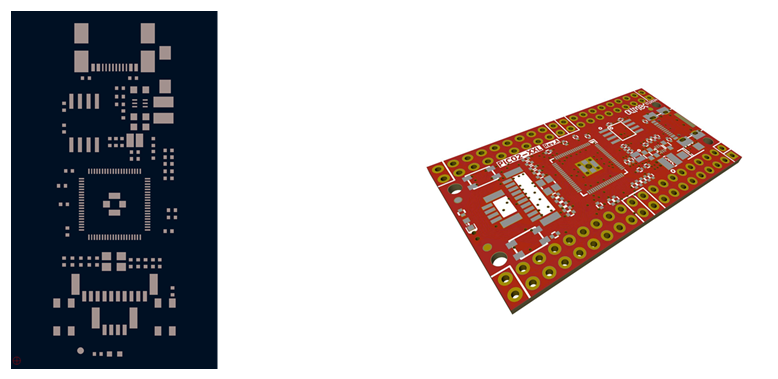
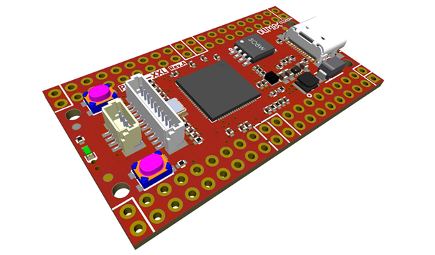
After this the PCB goes through the assembly process and we get the final PCB as below
Types of PCB
Most common ones are rigid PCBs, in this there are many types, single sided, double sided and multilayer pcb. The cost is higher for multilayer PCBs, and even higher if buried and or blind vias are used. Only the number of copper layers increase, rest of the layers on the top and bottom remain the same as discussed before.
Next is flex PCB (eg. FPC cables or ribbon cables), these are flat cables that connect two rigid PCBs. Or these can have components on it too. But it’s not recommended. These are mostly used as cables or small antennas for NFC
Then there is a rare type called rigid flex, in which the rigid and the flexible part are made as a single PCB. which is used when there is a big constraint on space, like in earphones, where the PCB is folded to occupy space in 3D.
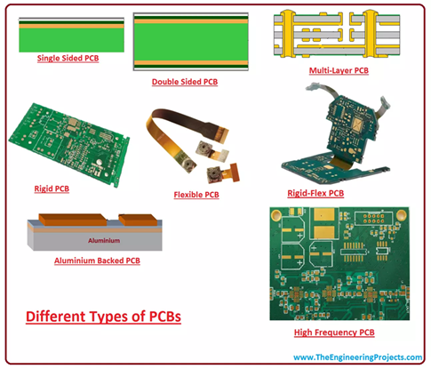
All these fancy types of PCB are designed with the same CAD package used for designing rigid boards. For Flex PCB, there is extra documentation needed, for example where the strong retainer should be placed, especially
Design Process Overview
It begins with drawing the circuit diagram in a CAD program like (KiCAD, Altium, Cadence), there are some best practices for schematic design, but I will discuss more some other time.
For schematic design, I’ll say this, if you are coming from a software background, treat the schematic design as your main file. You wouldn’t have all the functions in the same main file, you’d have functions in separate files, same way, I break down the project into smaller functions, and put them on separate schematics. Later on when you want to design, you can reuse these functions, examples would be like SD card, USB connectors, Power supply section, Lipo battery chargers, ethernet the list goes on. Similar things can be done for layouts too. Say there is a microcontroller you use often, you can make the schematic and the layout and reuse it in your new project. How to do this depends on the cad packages.
The next step is the PCB layout, one of the most important things in this process is not the routing of the board, but is the placement. Proper placement of the connectors, LEDs, Buttons, This also takes into account the MCAD requirements, like cutout for ports, like power in, ethernet, HDMI and such.
After the placement is planned, the next is to define the design rules as per the requirements and board manufacturers capabilities. Defining trace and space between the traces. Assigning net classes to power nets to make sure they can carry the sufficient current without burning the traces.
Then the next part is connecting the parts together with traces. Vias are used to go to different layers, there are also various kinds of Vias, the more complex, the higher the cost of the PCB.
The final step is gerber generation. There is a new format that came out a couple of years ago called the X2, this has some more information about the nets on the traces, but many manufactures are still on the old standard, the old standard is just art work.
To save some cost and for faster assembly, many designs are placed on a single board, assembled, and later broken down into single PCBs. These could be separated using V-cut or V-score.
Next, I want to talk about documentation. This is very important and often overlooked, Gerbers and drill files are not enough, if you want a smooth production run, your documentation must have all the information the manufacturer needs. I’ve talked about this in my other blog post here
Another design consideration you should keep in mind is the type of components used, SMD, through hole or there is a mix of the two types. Having both the types of components is usually higher cost than just having a single type as the board needs to go through two assembly steps, one for SMD and other for through hole components.
Sometimes, there is a part of a circuit you are not sure that it will work, you can use optional components like 0 ohm resistors to bypass a part of the circuit.
Design considerations
While designing the PCB, one must keep in mind the capabilities of the manufacturer. For example, the CAD packages will allow you to draw the thinnest trace of 0.5 mil, but this could be too thin to manufacture by the fab. Same goes for the space between two traces. These limitations should be defined as rules in CAD packages.
Think about repairing, keep plastic connectors away from smd components. When doing rework with hot air, the plastic melts, and damages the part.
Special care must be taken with the footprint of 3 pin devices like mosfets, transistors, crystals etc. The pinout for these components is not standard, some packages have a gate on pin 1, others on 2 or 3.
When you are starting out, make sure to add a lot of test points in the PCB. These allow you to probe the signals very easily, and these don’t cost anything. At Least you must add these on all power rails, to check if the board is powered up properly.
Make your own footprints and library, instead of downloading them. Use 3D models, to make sure of the sizes, as an extra step for verification and also make the pcb look good. Over time your library of components will increase and you will be more confident in using them, as they have been used in real PCBs.
One more important thing is to have same measurement unit in the footprint designer and the PCB designer.
SMD components sometimes tend to tombstone during assembly, and should use thermal relief for fixing it.
Chances are, there will be a couple of versions of the board, it’s very important to have your files in a version control system, and also you must label the version on your board.
For selecting components try using 1% resistors rather than 5%.
Also selecting connectors between through hole vs SMD. The Through hole is more durable than SMD. But if it’s not gonna be used a lot, you can use SMD as it’s easy to assemble and rework.
Footprints
Footprint is the area where the component is placed on the PCB. There is an IPC standard for drawing the footprint for various components. A footprint can come in three versions, based on the density of components on board, low density, medium density and high density, the footprints for the same component will have pad sizes from big to small respectively. There are IPC standards for footprint definitions, some CAD packages come with a wizard that helps in creating IPC standard compliant footprints.
Design tools
There are open source and commercial tools available discussed below
KiCAD
This is one of the most popular open source tools available, and you can design simple boards and complex boards in this tool. It has matured a lot in the last couple of years.
Altium Designer
This is the one I use personally. It offers better features than KiCAD, for example, much better constraints manager, impedance rules generation, more in depth design rules definitions. It also has a powerful query system for selection.
Eagle/Fusion 360
I manufactured exactly one PCB using this tool. I never got a hang of this, this tool will soon be merged into fusion 360.
Allegro
This is one of the most expensive tools, and used in the design of very complex stuff like server boards, etc, it has more features than Altium.
But these are just tools, just like having a great knife doesn’t makes one a good chef. Use the one that helps you get the job done.
Key Considerations in PCB
There are three key areas to consider when designing PCB, these are the electrical, mechanical and thermal, we will discuss all in detail below.
Electrical Considerations
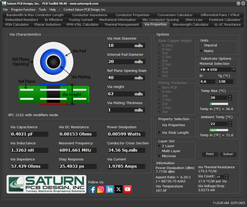
Coming back to PCB, using Saturn pcb toolkit is a must. It’s incredible such a tool is available for free. This tool uses the latest IPC standards for calculations, so you don’t need to buy these expensive standards. There are many calculators present in it. Most used ones are trace width calculator, current capacity of vias, characteristic impedance, etc.
When doing high layer count PCB, you must make sure the manufacturer understands what exactly you need in the design.
High speed design considerations
This is a whole topic on its own, but if you are starting out, start with a board that has one high speed connection vs multiple with different impedance profiles, learn about transmission line, reflections and ground return paths, etc. these are some of the key words to get started.
Mechanical Considerations
There must be a way of mounting the pcb. The most common one is to use screws. This requires holes on the PCB. If the PCB needs to be grounded with the mechanical box, the hole must be copper plated and connected to the PCB ground, if its a plastic enclosure, non plated hole would also suffice.
Another type of mounting type is by snapping it in the plastic enclosure using tabs. For this you need to make sure the area where the tabs will be present has enough clearance.
If you are starting with an enclosure in mind, you have to make sure the board dimensions match, along with all the holes for mounting the PCBs.
Another very important mechanical consideration is the connectors. Not only do you have to make sure the connectors are separated on the PCB, but also, you need to make sure the width of the connector wire will not interfere with the neighbouring connector.
Thermal Considerations
Unless it’s a low power device, there are many sources of heat on a PCB. Power supplies( especially linear ones), resistors, motor drivers, switching inductors. To mitigate this, you could heat sinks, dissipate the heat in the power or ground planes. This can be done with via stitching or having just a thermal pad on the bottom of the pcb.
Design for manufacturing
Avoid chance of tombstoning, this happens when one side of the footprint has a large copper area and the other side is a trace.
Make sure there are no errors in the DRC.
Prototyping and testing
Before the cheap PCB services were available, there were Diy ways of making PCBs at home, using various methods like using photoresist PCB, toner transfer, etc, and then using some hazardous chemicals to etch away the copper.
I don’t recommend these methods now, nowadays the PCB manufacturing cost has come down so much, there is literally no benefit of using DIY methods. Plus you get a professionally made and tested PCB.
Testing PCB happens at various stages of assembly, the manufacturer will test the board just for connectivity. After the PCB is assembled, you have to perform functional testing.
Trends
These days there are certain tools that use AI in electronics design, there are tools that work at different stages of design, there is one called circuit mind, this helps to make many design alternatives, and depending on what you are trying to optimize.
Then there is Kady, this is useful when you have finished your design, and is useful for BoM optimization and making use of any incompatible components.
Another one is Flux AI, this I think helps with the layout.
I haven’t used them personally, and I think they need to be a little bit more mature before you can start using them.
There chat gpt ofcourse for queries and learning some concepts.
Well, I hope you found this post useful.
Fin.
If you want to see the live video on this check it out here
Also if you want to keep the conversation going join us at DevHeads discord
No part of this post was generated using LLMs or diffusion models.
Archives
Tags